03. Environment Setup & Testing
| Owner | M. G. Sadek |
|---|---|
| Tags |
01 - Objective
In this Lab tutorial, we will learn how to install software tools required to develop, simulate and test VHDL code, also those required to upload the compiled code to the FPGA hardware.
At the end of this tutorial you should have the required software tools and have good understanding of how to create a project from scratch, add VHDL code, perform pin assignment, compile and upload the compiled code to the hardware FPGA and test it.
02 - Downloads:
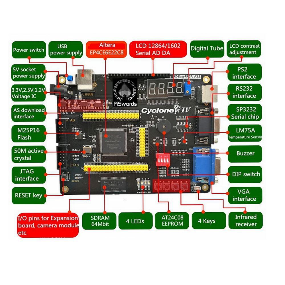
- Altera Cyclone IV Development board pin information: Altera-Cyclone-IV-board-V3.0/Hardware documentation at master · jvitkauskas/Altera-Cyclone-IV-board-V3.0 (github.com)
03 - Preparing Developing Environment:
Step1: Installation:
- Download & install the appropriate software applications from the following link: Intel® Quartus® Prime Lite Edition Design Software Version 21.1 for Windows
- You can follow the steps in this video for download and installation: Downloand and Install Quartus Prime Lite 20.1 on Windows 10 - YouTube
- Make sure to download these files:
- Make sure to put all downloaded files in the same directory then run the
QuartusLiteSetupfile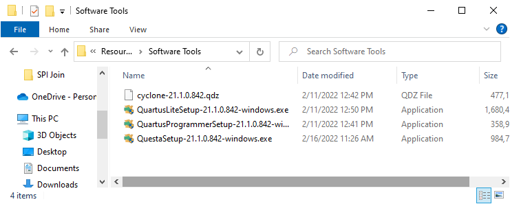
- To install
QuartusLiteSetup,QuartusProgrammerSetupandQuesta - Intel FPGA Starter Edition, select the required installations as in the following image.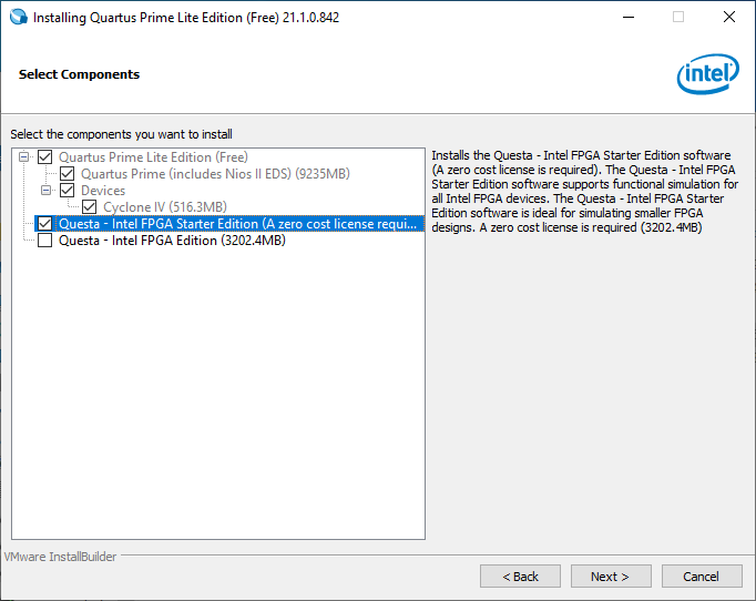
- After installation finishes, select
Run Blaster II programmer driver installationto install drivers required by the Blaster II programmer.
Step2:
- After successfully installation and installing the drivers, connect the USB Blaster and follow the steps in this wiki to install the compatible drivers:
Altera USB Blaster Driver Installation Instructions - Terasic Wiki
💡Warning: Do not insert to remove the USB Blaster ribbon cable while the device is powered on. There was an included warning that the board would likely be damaged. I did not test this.Steps summary:
Source: GoJimmyPi: First FPGA Test Drive with Altera Cyclone IV
- Plug the USB-Blaster II cable into your PC.
- Open the Device Manager, and right-click on the Unknown device under the Other devices branch.
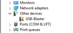
- Select Update Driver Software.
- Select Browse my computer for driver software.
- Enter the location of the Quartus Prime software USB-Blaster II driver files directory (<Path to Quartus Prime installation>\drivers\usb-blaster-ii) in the Search for driver software in this location field.
- Click Next.
- Click Install in the Would you like to install this device software? Windows security dialog box.
- Close the Update Driver Software - Altera USB-Blaster II (Unconfigured) successful installation notification. The Device Manager now shows a new branch called JTAG cables with an Altera USB-Blaster II (Unconfigured) node.
- Open the Quartus Prime Programmer. Within a few seconds, the JTAG cables branch displays two nodes: Altera USB-Blaster II (JTAG interface) and Altera-USB Blaster II (System Console interface).
04 - Running your first test project:
Step1: Create a new project:
Source: Intel® Cyclone® 10 LP FPGA Board - How to Program Your First FPGA
- Run the Quartus Prime Lite Edition program.
- Open
Filemenu and selectNew Project Wizard.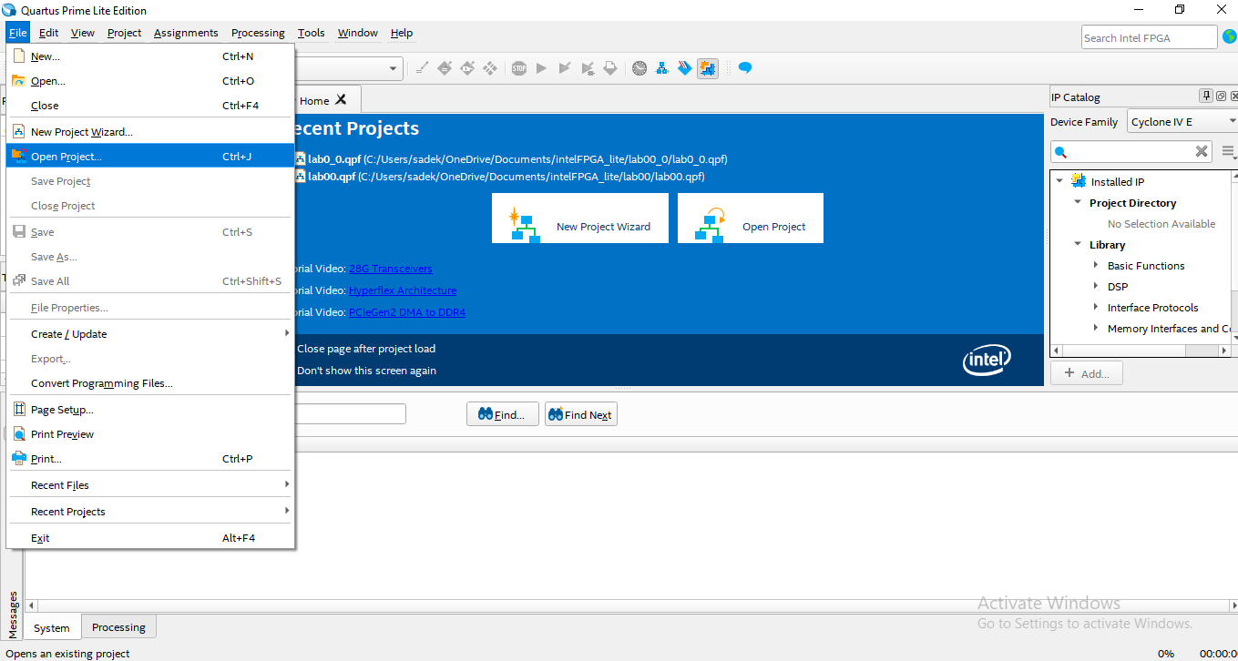
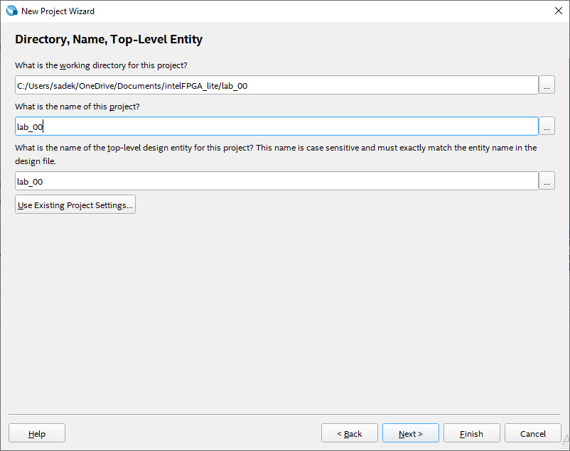
- You may need to press Next to move to the next window.
- Enter the directory for the project, a project name.💡Important: You must choose a read/write directory, such as Documents directory.
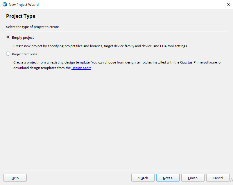
- Press Next and select am Empty Project, then press Next.
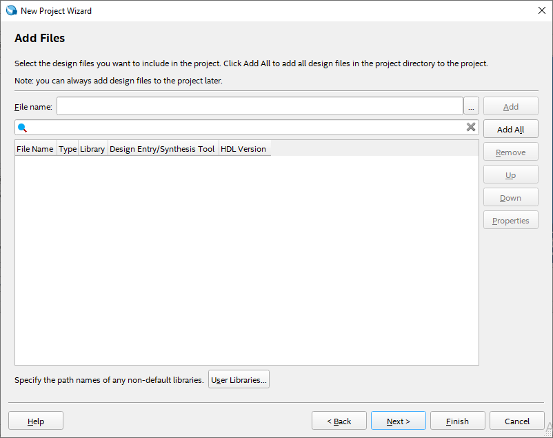
- We don’t need to add any files right now, so, we bypass the next window by pressing Next.
- Now, we need to select the device that we will use, our main chip is the ALTERA FPGA CycloneIV series
EP4CE6E22C8Nthe fourth generation. So, select the right chip and press Next.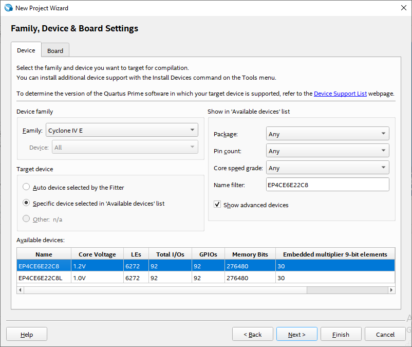
- We won’t change default tool settings, so, press Next. Or, we can select the desired simulation tool, choose
QuestaSimtool withVHDLformat.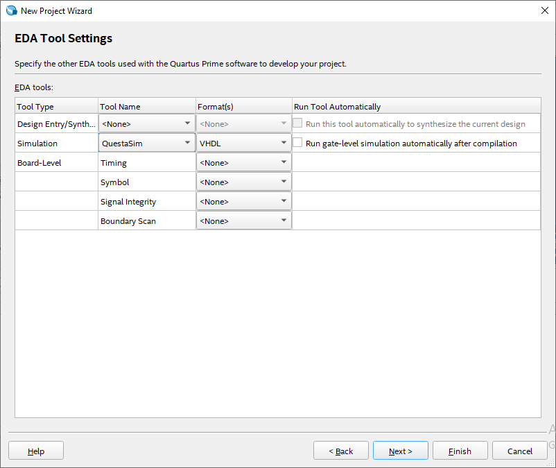
- A summary should be shown.
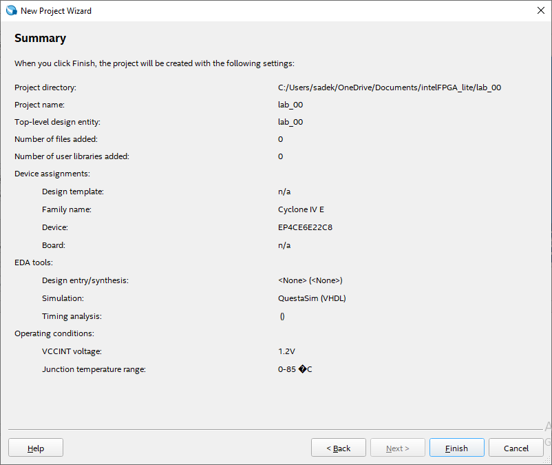
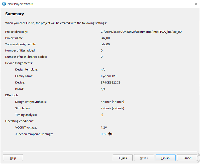
- Now, press the Finish button to finish creating our new project.
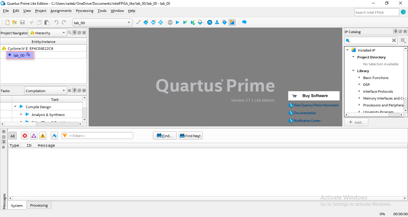
- Our project should be shown in the Project Navigator
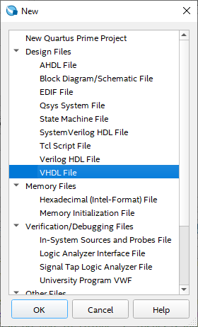
Step2: Adding a new VHDL File to your project:
- From
Filemenu, chooseNew.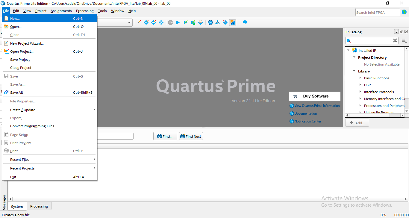
- In the
Newdialog window, underDesign Files, selectVHDL Fileand pressOK.
Step3: Entering VHDL code:
- Now, enter your code into the text editor area.
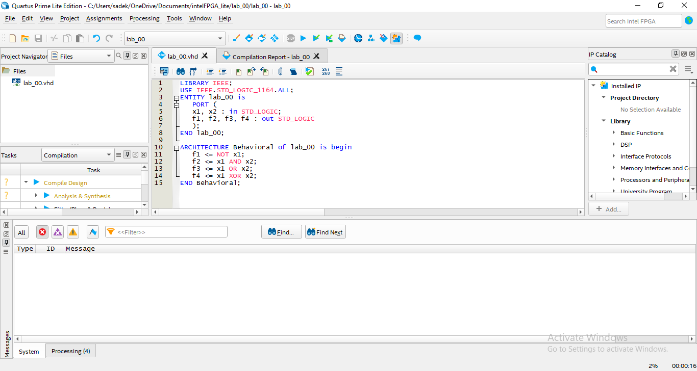
- Sample Code:
LIBRARY IEEE; USE IEEE.STD_LOGIC_1164.ALL; ENTITY lab_00 is PORT ( x1, x2 : in STD_LOGIC; f1, f2, f3, f4 : out STD_LOGIC ); END lab_00; ARCHITECTURE Behavioral of lab_00 is begin f1 <= NOT x1; f2 <= x1 AND x2; f3 <= x1 OR x2; f4 <= x1 XOR x2; END Behavioral;💡Important: In VHDL, theEntityname must be the same as the project name, otherwise, you have to add the new entity as the top-level entity of the project [Tutorial to add the new entity as the top-level: Intel Quartus Prime Tutorial Part 6 | Error Top-level design entity "name" is undefined - YouTube]
- Sample Code:
- Then, save the file and name it.
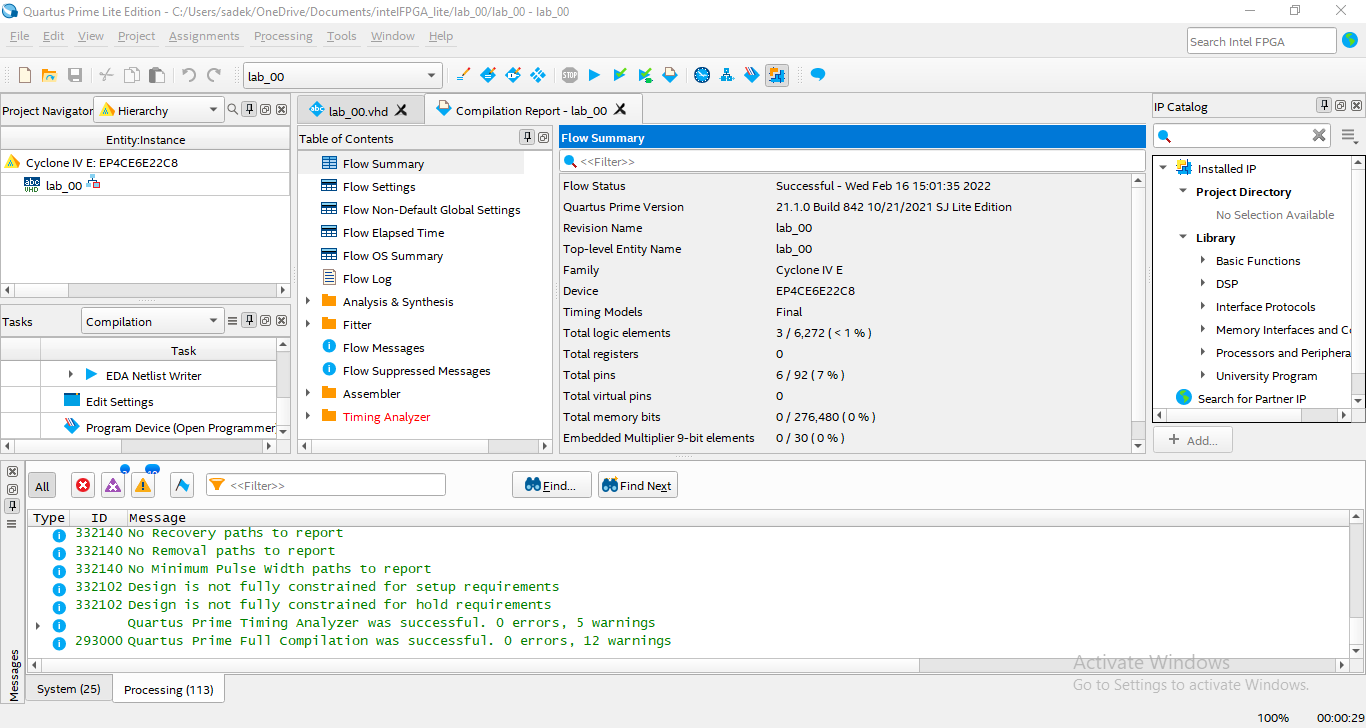
Step4: Pin Assignment & Compiling:
- To compile the project, open the menu
Processingand pressStart Compilation.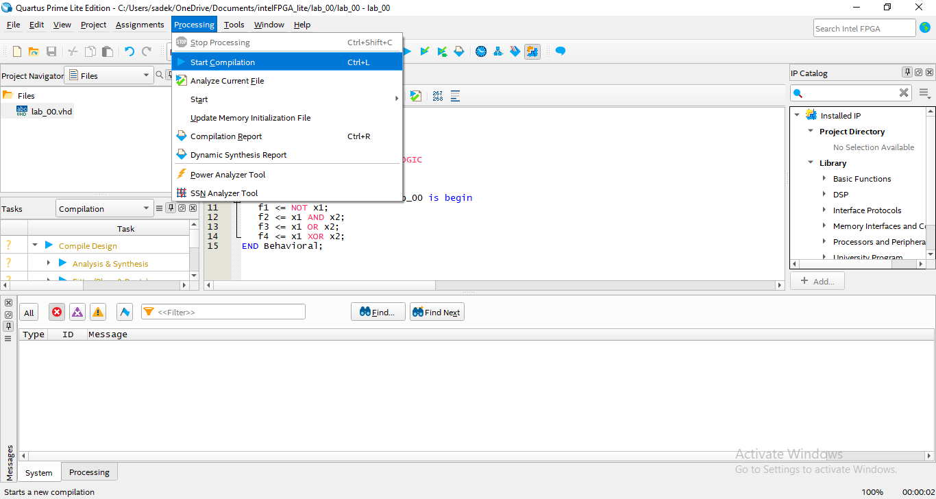
- While the pins are not actually assigned, there will be a compiler warning, telling that no pins are assigned for input/output pins used.
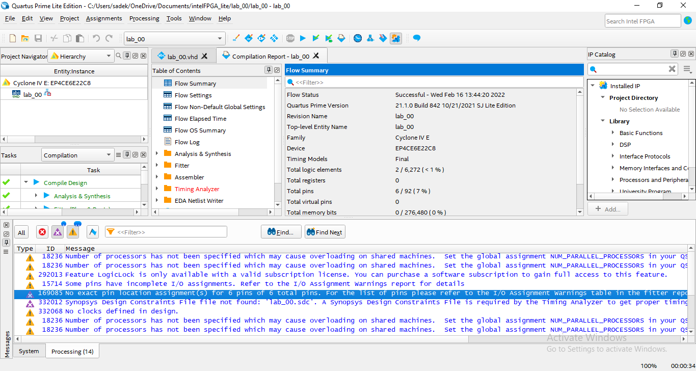
- While the pins are not actually assigned, there will be a compiler warning, telling that no pins are assigned for input/output pins used.
- Click on
Assignmentsmenu and selectPin Planner.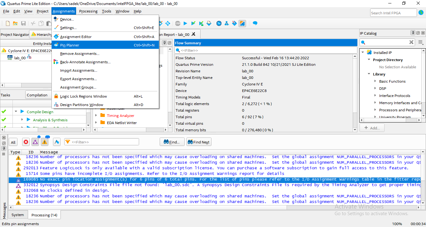 💡Important: we must have explicitly assigned our chip part number, otherwise this feature is not available
- Double-click in the Location column in front of each input/output pin, a drop-down list will appear.
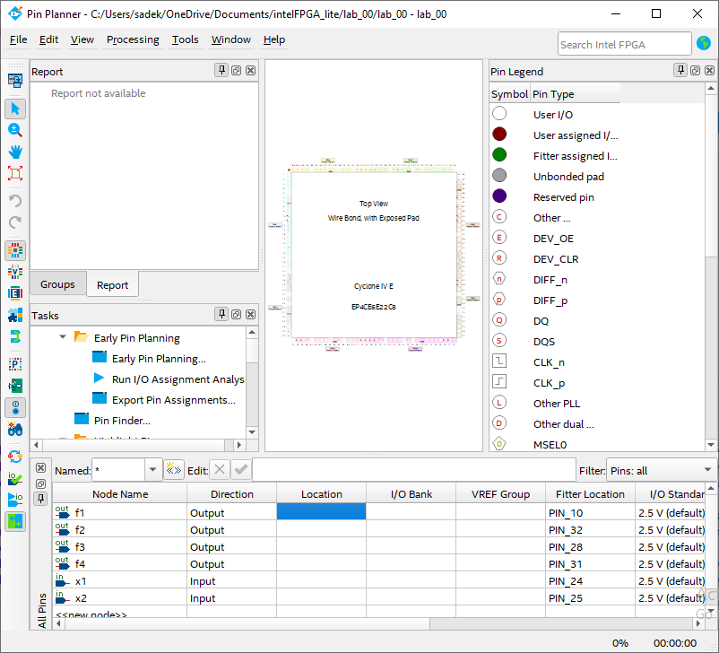
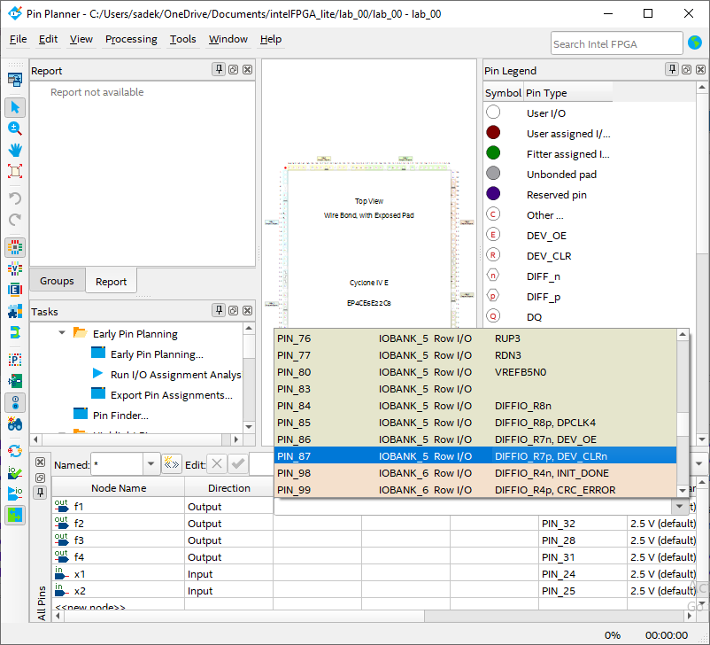
- We need to assign the pins to push buttons and LED as shown in the schematic:
- Altera Cyclone IV Development board pin allocation table:
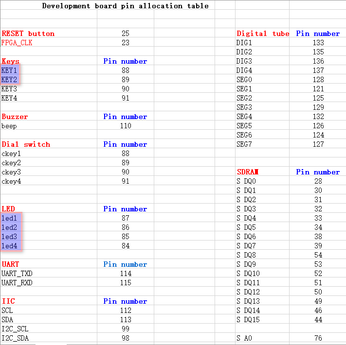
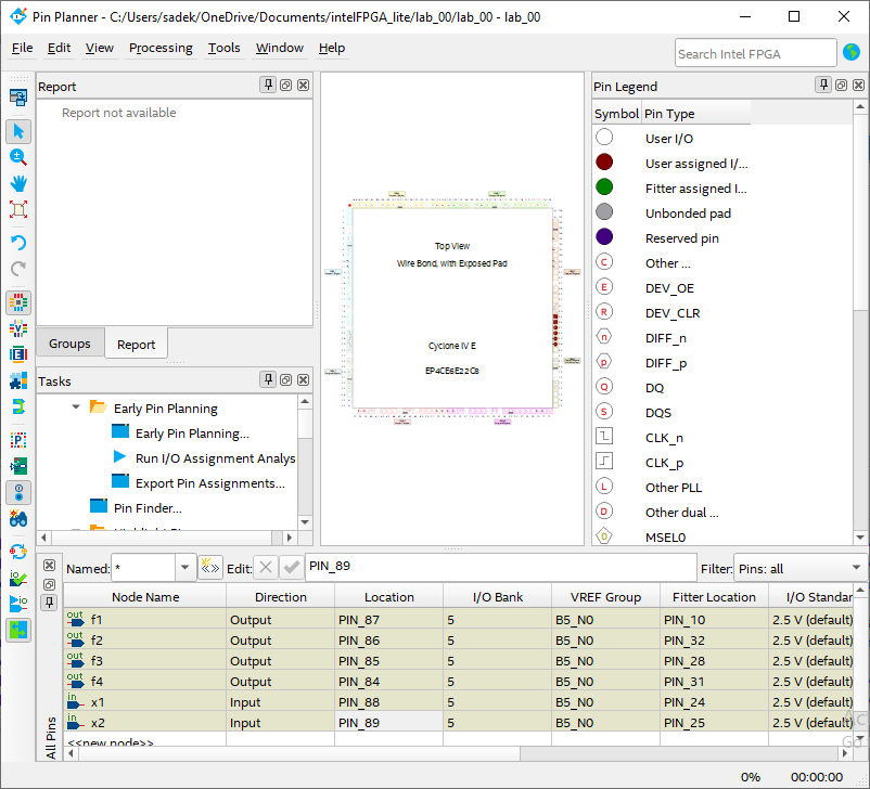
- Altera Cyclone IV Development board pin allocation table:
- Now, close the Pin Planner and compile again.
Step5: Visual verification of the design:
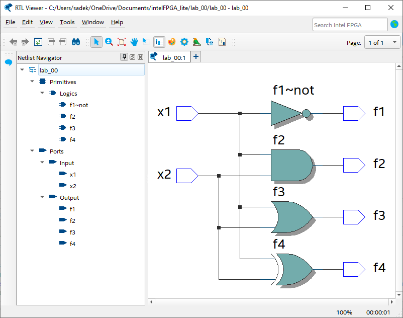
- We can show the circuit implemented by our VHDL code using RTL view. From
Toolsmenu, openNetlist Viewersand selectRTL viewer.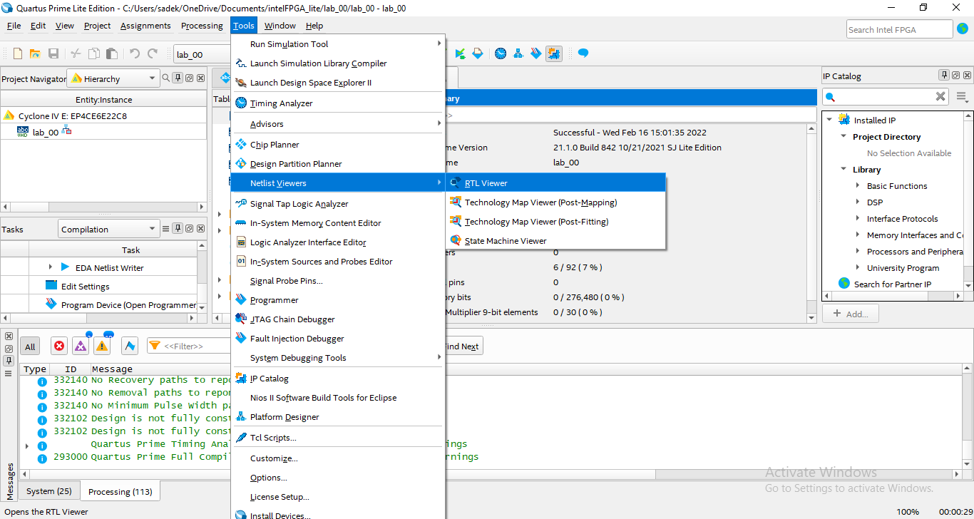
- The circuit gates, input/output pins and connections will be displayed as following:
Step6: Uploading the compiled code to the FPGA hardware:
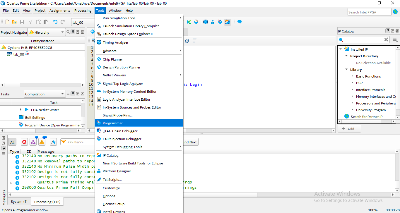
- Finally, we're ready to send the FPGA code to our device. To Program the FPGA kit: Click
Toolsmenu then selectProgrammer.
- To send the FPGA code to the device, select "
Processing-Start" (or simply press the "Start Button").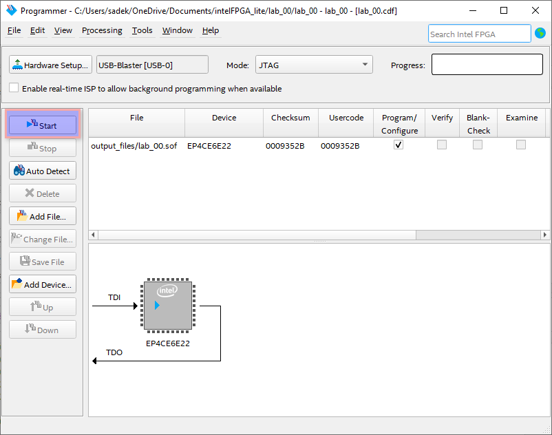
- If successful, there will be an indication in the progress box.
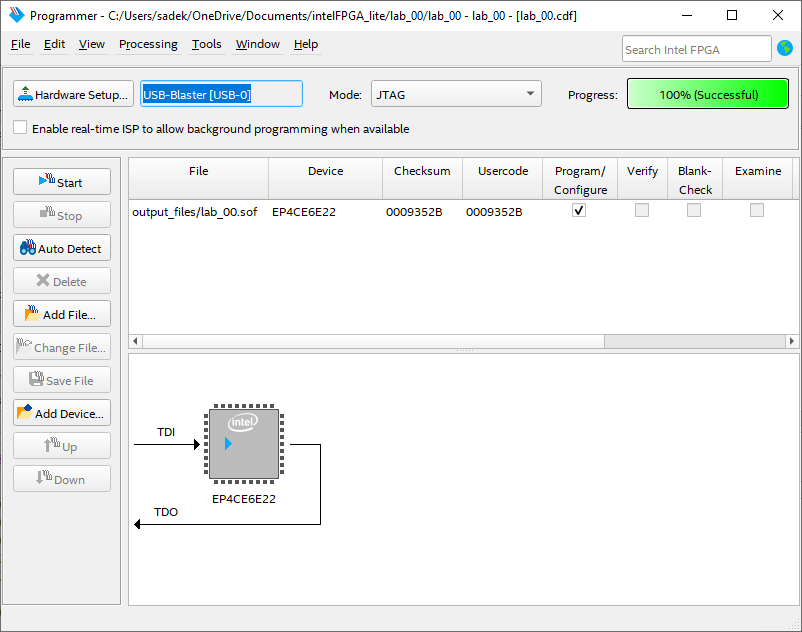
- That's it! There's now 4 gate programmed in the FPGA. Press S1 or S2 to have the corresponding LEDs ON or OFF verifying the 4 gates.
Important Notes:
So, we can use the following code instead, to provide the same behavior for the desired gates in a user-friendly manner.
LIBRARY IEEE;
USE IEEE.STD_LOGIC_1164.ALL;
ENTITY lab_00 is
PORT (
		x1, x2 : in STD_LOGIC;
		f1, f2, f3, f4 : out STD_LOGIC
	);
END lab_00;

ARCHITECTURE Behavioral of lab_00 is begin
	f1 <= NOT x1;
	f2 <= NOT(NOT x1 AND NOT x2);
	f3 <= NOT(NOT x1 OR  NOT x2);
	f4 <= NOT(NOT x1 XOR NOT x2);
END Behavioral;