04. Logic Gates Simulation & Real-Time
| Owner | M. G. Sadek |
|---|---|
| Tags |
01 - Objective
In this Lab tutorial, we will reimplement lab-00 to get you familiar with the VHDL development process.
02 - Logic Gates Implementation
First, we need to create a project as mentioned in lab-03 then in the Entity we will define two primary inputs which are A and B besides defining an output signal for each gate (f1, f2, f3, f4). But before we do this we need to include some IEEE packages which are
library IEEE;
use IEEE.STD_LOGIC_1164.ALL;
then we can define our Entity as
entity lab01 is
	port ( A, B: in STD_LOGIC;
        f1, f2, f3, f4: out STD_LOGIC
			 );
end lab01;

-- Note that each output signal will hold the gate's output.,
Now we need to define the behaviour by describing the architecture
architecture Behavioral of lab01 is
begin
    f1 <=   NOT A;  -- NOT_GATE
    f2 <= A AND B;  -- AND_GATE
    f3 <= A OR  B;  -- OR_GATE
    f4 <= A XOR B;  -- XOR_GATE
end Behavioral;
03 - Simulation Process
In order to test your design, you must develop a test bench for it. The purpose of the test bench is to prepare the input values and check on the output then raise an alert upon output mismatch. Note that creating a test bench is similar to creating any VHDL design component but the difference is that its entity is empty.
library IEEE;
use IEEE.STD_LOGIC_1164.ALL;

entity lab01_tb is
end lab01_tb;
Now its time to set our inputs values:
architecture testing_lab01_tb of lab01_tb is

	-- First we need to define the unit under test
  component lab01
		port ( A, B: in STD_LOGIC;
        f1, f2, f3, f4: out STD_LOGIC
			 );
	end component;

-- Then define the input signals
signal a, b, of1, of2, of3, of4 : STD_LOGIC;


-- And finally we need to map those signals to the components inputs
begin
	lab01_0 : lab01 port map(a, b, of1, of2, of3, of4);

	-- We need to define the input values inside a process in order to have
  -- a sequential execution.
	process
	begin
	  a <= '0';
	  b <= '0';
		wait for 10 ns;

	  a <= '0';
	  b <= '1';
		wait for 10 ns;

	  a <= '1';
	  b <= '0';
		wait for 10 ns;

	  a <= '1';
	  b <= '1';
		wait for 10 ns;
	end process;
end testing_lab01_tb;
After you develop the test bench, you need to check its syntax for any errors. To do so, please run
$ ghdl -s lab01.vhdl
$ ghdl -a lab01.vhdl
$ ghdl -s lab01_tb.vhdl
$ ghdl -a lab01_tb.vhdl
the -s option checks for syntax error and if no message has appeared then your syntax is correct. The next step is to create the simulation waveform, and in order to do so, you need to elaborate the design then run a simulation on the test bench.
$ ghdl -e lab01_tb
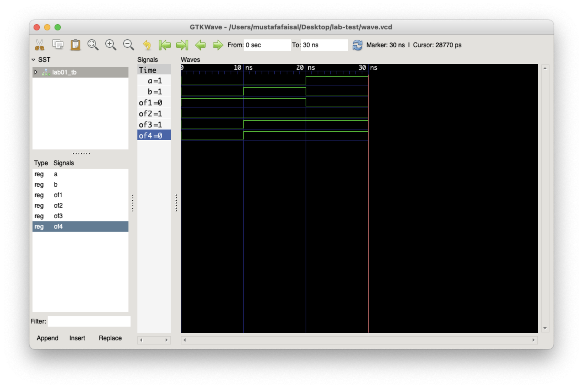
$ ghdl -r lab01_tb --vcd=output_waveform.vcd --stop-time=1000nsAfter the simulation finishes you will find the generated waveform file with the name output_waveform.vcd in your directory which you will open it using gtkwave application.
04 - Flashing Process
- VHDL script is changed to following script, to overcome LEDs active LOW and push buttons pull-up resistors design
library IEEE;
use IEEE.STD_LOGIC_1164.ALL;
use IEEE.STD_LOGIC_ARITH.ALL;
use IEEE.STD_LOGIC_UNSIGNED.ALL;
entity lab01 is
port ( A, B: in STD_LOGIC;
	f1, f2, f3, f4: out STD_LOGIC
);
end lab01;
-- Note that each output signal will hold the gate's output.,
architecture Behavioral of lab01 is
begin
f1 <=   NOT A;  -- NOT_GATE
f2 <= NOT(NOT A AND NOT B);  -- AND_GATE
f3 <= NOT(NOT A OR  NOT B);  -- OR_GATE
f4 <= NOT(NOT A XOR NOT B);  -- XOR_GATE
end Behavioral;- Please follow the same steps found in
lab-03in order to synthesise and flash the FPGA.
05 - Output Verification
- State 0: A: LOW [Free] - B: LOW [Free]
B A NOT AND OR XOR 0 0 1 0 0 0 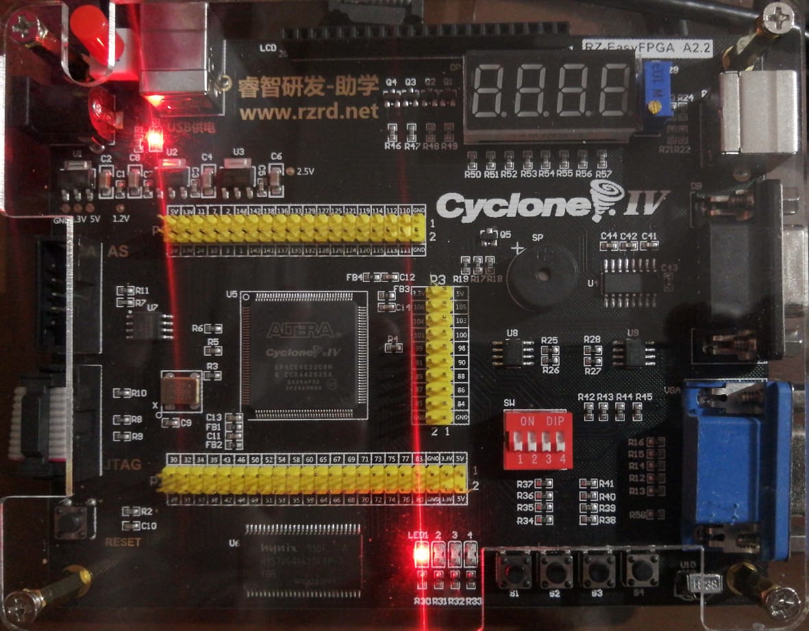
- State 1: A: HIGH [Pressed] - B: LOW [Free]
B B NOT AND OR XOR 0 1 0 0 1 1 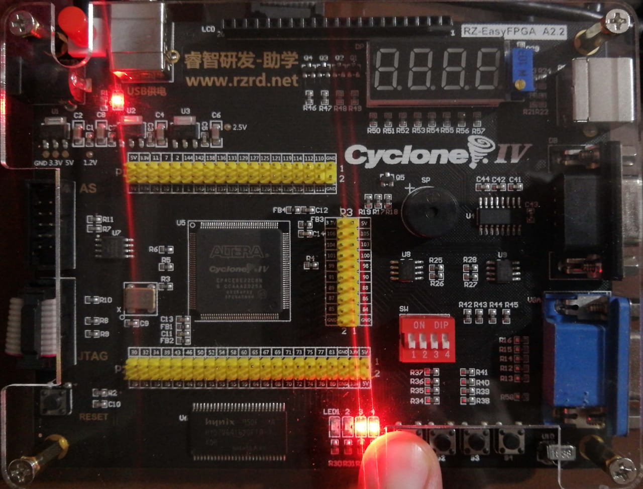
- State 2: A: LOW [Free] - B: HIGH [Pressed]
B A NOT AND OR XOR 1 0 1 0 1 1 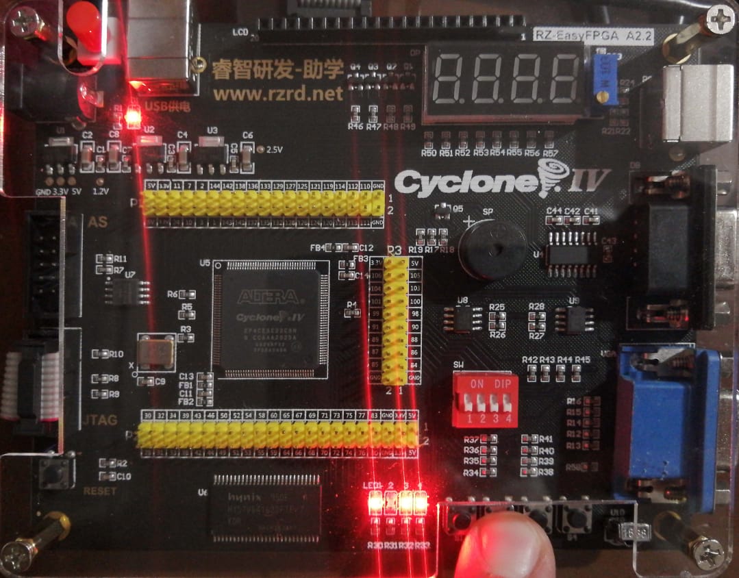
- State 3: A: HIGH [Pressed] - B: HIGH [Pressed]
B A NOT AND OR XOR 1 1 0 1 1 0 .jpeg)