09. 8-bit Register
| Owner | M. G. Sadek |
|---|---|
| Tags |
Parent Page: Digital Logic Design - Lab Tutorials
01 - Objective
In this tutorial, we discuss building an 8-bit register.
02 - Logic Gates Implementation
The following code defines an 8-bit register entity, which takes in a clock signal, a reset signal, an enable signal, and an 8-bit input data signal. It outputs the input data signal whenever the enable signal is high.
-- 8-bit Register VHDL code
library ieee;
use ieee.std_logic_1164.all;
entity register_8bit is
port (
clk : in std_logic;
reset : in std_logic;
enable : in std_logic;
data_in : in std_logic_vector(7 downto 0);
data_out : out std_logic_vector(7 downto 0)
);
end entity register_8bit;
architecture behavioral of register_8bit is
begin
process (clk, reset)
begin
if reset = '1' then
data_out <= (others => '0');
elsif rising_edge(clk) then
if enable = '1' then
data_out <= data_in;
end if;
end if;
end process;
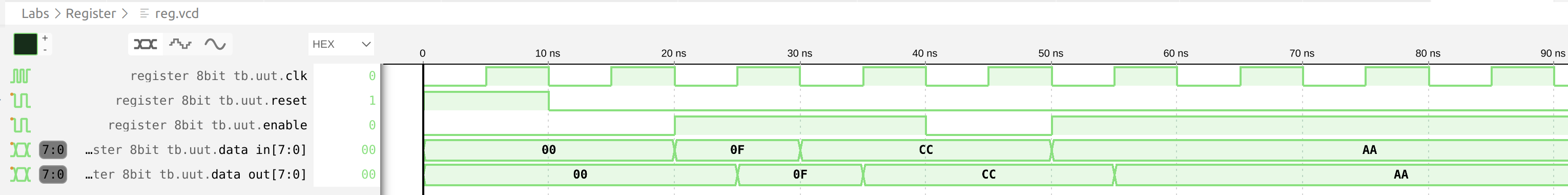
end architecture behavioral;The testbench includes a clock process that generates a clock signal with a period of 10 ns. It also includes a stimulus process that provides input signals to the register entity. Initially, the reset signal is high and the enable signal is low. After 10 ns, the reset signal is set low and the enable signal is set high, and the input data is set to "00001111". After another 10 ns, the input data is changed to "11001100". Then, the enable signal is set low.
-- Testbench for 8-bit Register

library ieee;
use ieee.std_logic_1164.all;

entity register_8bit_tb is
end entity register_8bit_tb;

architecture behavioral of register_8bit_tb is
  component register_8bit
    port (
      clk : in std_logic;
      reset : in std_logic;
      enable : in std_logic;
      data_in : in std_logic_vector(7 downto 0);
      data_out : out std_logic_vector(7 downto 0)
	  );
  end component;

  signal clk : std_logic := '0';
  signal reset : std_logic := '0';
  signal enable : std_logic := '0';
  signal data_in : std_logic_vector(7 downto 0) := (others => '0');
  signal data_out : std_logic_vector(7 downto 0);

begin
  uut : register_8bit
    port map (
      clk => clk,
      reset => reset,
      enable => enable,
      data_in => data_in,
      data_out => data_out
    );

  clk_process : process
  begin
    clk <= '0';
    wait for 5 ns;
    clk <= '1';
    wait for 5 ns;
  end process;

  stim_proc : process
  begin
    reset <= '1';
    enable <= '0';
    data_in <= (others => '0');
    wait for 10 ns;
    reset <= '0';
    wait for 10 ns;
    enable <= '1';
    data_in <= "00001111";
    wait for 10 ns;
    data_in <= "11001100";
    wait for 10 ns;
    enable <= '0';
    wait for 10 ns;
    enable <= '1';
    data_in <= "10101010";
    wait for 10 ns;
    wait;
  end process;
end architecture behavioral;
03 - Simulation Process
04 - Flashing Process
Please follow the same steps found in lab-03 in order to synthesize and flash the FPGA.