10. 8-bit Shift Register
| Owner | M. G. Sadek |
|---|---|
| Tags |
Parent Page: Digital Logic Design - Lab Tutorials
01 - Objective
In this tutorial, we discuss building an 8-bit Right shift register [Serial to parallel].
02 - Logic Gates Implementation
The following code defines an 8-bit shift register entity, which takes in a clock signal, a reset signal, and 1-bit input data signal. It outputs the input data signal after shifting it to the right, whenever the clock rises to high.
-- 8-bit shift register with a left shift operation.
-- This code defines a shift register entity with one 8-bit input,
-- one output, and a clock input.
-- The shift register is synchronous,
-- meaning that it shifts its contents only on the rising edge of the clock signal.
-- 1-bit to 8-bit shift register with serial input and parallel output
library ieee;
use ieee.std_logic_1164.all;
entity shift_register is
port (
clk : in std_logic; -- clock input
reset : in std_logic; -- asynchronous reset input
serial : in std_logic; -- serial input
parallel: out std_logic_vector(7 downto 0) -- parallel output
);
end entity;
architecture Behavioral of shift_register is
signal shift_reg : std_logic_vector(7 downto 0); -- shift register
begin
process(clk, reset)
begin
if reset = '1' then
shift_reg <= (others => '0'); -- reset to all zeroes
elsif rising_edge(clk) then
shift_reg <= serial & shift_reg(7 downto 1);
end if;
end process;
parallel <= shift_reg; -- output the parallel register
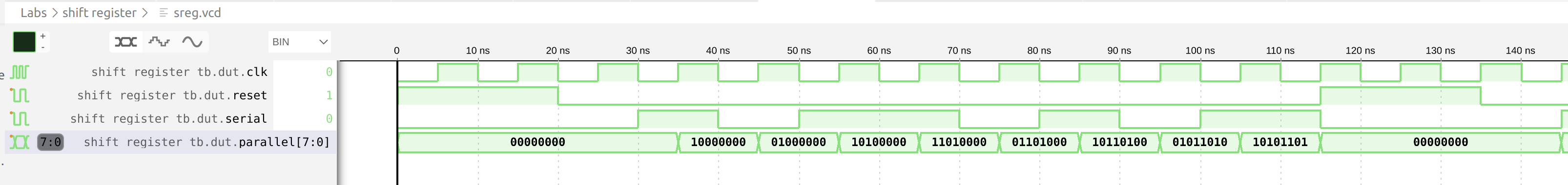
end architecture;The testbench includes a clock process that generates a clock signal with a period of 10 ns. It also includes a stimulus process that provides input signals to the register entity. Initially, the reset signal is high. After 20 ns, the reset signal is set low, and the input serial data is fed to the serial input.
-- Testbench for 8-bit Shift Register
library ieee;
use ieee.std_logic_1164.all;

entity shift_register_tb is
end entity;

architecture Behavioral of shift_register_tb is
  component shift_register is
    port (
      clk     : in  std_logic;
      reset   : in  std_logic;
      serial  : in  std_logic;
      parallel: out std_logic_vector(7 downto 0)
    );
  end component;

  signal clk      : std_logic := '0';
  signal reset    : std_logic := '0';
  signal serial   : std_logic := '0';
  signal parallel : std_logic_vector(7 downto 0);

begin
  dut : shift_register
    port map (
      clk      => clk,
      reset    => reset,
      serial   => serial,
      parallel => parallel
    );

  -- clock generation
  clk_gen : process
  begin
    while true loop
      wait for 5 ns;
      clk <= not clk;
    end loop;
  end process;

  -- test sequence
  test_seq : process
  begin
    reset <= '1';  -- reset the shift register
    serial <= '0'; -- initial input value
    wait for 20 ns;
    reset <= '0';  -- release reset
    wait for 10 ns;

    -- shift in '1'
    serial <= '1';
    wait for 10 ns;

    -- shift in '0'
    serial <= '0';
    wait for 10 ns;

    -- shift in '1'
    serial <= '1';
    wait for 10 ns;

    -- shift in '1'
    serial <= '1';
    wait for 10 ns;

    -- shift in '0'
    serial <= '0';
    wait for 10 ns;

    -- shift in '1'
    serial <= '1';
    wait for 10 ns;

    -- shift in '0'
    serial <= '0';
    wait for 10 ns;

    -- shift in '1'
    serial <= '1';
    wait for 15 ns;
  end process;
end Behavioral;
03 - Simulation Process
04 - Flashing Process
Please follow the same steps found in lab-03 in order to synthesize and flash the FPGA.